Share
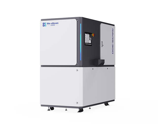
SEMNova-1000 High-Throughput (Field Emission) Scanning Electron Microscope
Still thinking? Feel free to consult us,Contact us!
Browse Similar Products
Label List
- Product Description
- Feature advantages
- Basic parameters
-
SEMNova-1000 High-Throughput (Field Emission) Scanning Electron Microscope
The SEMNova-1000 High-Throughput (Field Emission) Scanning Electron Microscope is designed for cross-scale large-scale sample SEM characterization and analysis, widely used in research and industry. Its automated ultra-high-speed nano imaging technology provides you with an extraordinary imaging experience.
Product Introduction
The SEMNova-1000 High-Throughput (Field Emission) Scanning Electron Microscope, independently developed by Borui and possessing independent intellectual property rights, achieves high-throughput imaging through systematic innovative design in imaging technology, motion platform, circuit control, and intelligent algorithms, with imaging speeds exceeding traditional electron microscopes by dozens of times. It adopts a technology solution that uses direct electron detectors, successfully overcoming the limitations of traditional SEM technology in speed, accuracy, and sample damage, revolutionizing the scanning electron microscope from a traditional nano "camera" to a nano "video camera." It is also easy to operate, with fully automated one-click sample switching and 24/7 unattended operation, significantly enhancing research efficiency.
We apply mature industrial high-throughput electron microscope detection technology in fields such as life sciences, materials research, semiconductor industry, and geological resources. It has significant advantages, especially in applications such as 3D reconstruction in neurobiology, large-area characterization and analysis of materials, semiconductor reverse engineering, and nanotechnology analysis.
-
Product Advantages
● Comprehensive imaging speed > 10 times that of traditional electron microscopes
● Dual-channel synchronous imaging of secondary electrons and backscattered electrons
● Rapid generation of data analysis reports from massive SEM images
● Cross-scale material characterization from millimeters to nanometers
Product Features
1. Ultra-fast Imaging
●Achieved dual-channel synchronous imaging of secondary electrons and backscattered electrons through independently developed hardware and software design: video-level high-resolution imaging;
●High-definition video-level frame rate allows real-time observation of sample dynamic changes;
2. High Imaging Quality
●Unique immersion electromagnetic compound lens system effectively reduces optical aberrations of the objective lens at low landing energies, achieving extremely high resolution;
●Electrostatic scanning deflection system combined with the objective lens field greatly reduces image edge distortion compared to traditional electron microscope magnetic deflection systems, allowing for perfect images with both high resolution and large field of view;
●In-Lens SE and BSE semiconductor direct electron detectors enable dual-channel simultaneous high-speed imaging, with high sensitivity and high signal electron collection efficiency, achieving high image contrast and signal-to-noise ratio even under nA-level high beam current conditions;
●Equipped with an active compensation system (laser interference vibration compensation, electromagnetic interference active compensation) to eliminate environmental interference, ensuring high-resolution and high-quality imaging;
3. Cross-Scale Large-Scale Imaging
●Ultra-high-speed scanning imaging capability, combined with a fully automatic focusing tracking system and A.I. image processing algorithms, enables high-resolution fully automatic uninterrupted matrix scanning of ultra-large area samples, automatically stitching to obtain large-size nanometer-level resolution panoramic imaging, providing cross-scale information fusion capability, achieving cross-scale material characterization from nanometers to millimeters;
4. Intelligent Analysis
●Big data intelligent analysis, rapid generation of data analysis reports from massive SEM images;
●Intelligent image processing, customized image measurement, statistics, and analysis;
5. Simple Operation
●Fully automatic sample loading and navigation, one-click sample replacement, convenient operation, saving labor time. Large field optical imaging navigation seamlessly connects with SEM imaging, quickly and accurately locating and observing specified areas;
●24/7 fully automated unmanned operation capability.
-
Electron Optical Lens Electron Gun Schottky Type Thermal Field Emission Electron Source
Beam Current Stability <1%/day
Objective Lens System SORRIL™ Electromagnetic Compound Lens
Sample Stage Deceleration Mode
Resolution 1.5 nm @ 1kV 1.3nm @ 3kV
Immersion Electromagnetic Lens (*①)
Acceleration Voltage 0.1-12 kV
Continuously Adjustable (*②)
Magnification 500X~600,000X (SEM Image) 1X-600X (Optical Navigation)
Beam Current 50pA~30nA
(*③)
Standard Working Distance 1.5mm
Maximum Field of View 100um (Standard Working Distance) 1mm (Maximum Working Distance)
Electron Beam Blanker Electrostatic Blanker
Detector System Electron Detector
(Standard)
In-column SE Detector In-lens BSE Detector Working Distance Height Detection
Focus Tracking™ Automatic Focus Tracking System Optical Navigation Accuracy
15um Image Processor Minimum Imaging Dwell Time
10ns/pixel Fastest Imaging Flux
SE and BSE each 100M pixels/s Acquisition Method
Dual Channel Synchronous Acquisition SE+BSE Maximum Image Resolution
24kx24k pixels Image Averaging
Supports Point Averaging, Line Averaging, Area Averaging Sample Motion Platform Travel X=150mm, Y=150mm, Z=20mm
Maximum Sample Load 5kg
Repeat Positioning Accuracy (*) X=±3um, Y=±3um, Z=±50nm
(*④)
Drive Method
X/Y Piezoelectric Ceramic Drive Z Stepper Motor + Piezoelectric Ceramic Drive Standard Sample Holder 4~6 inch sample loading tray with pre-vacuum chamber automatic sample feeding
Optional loading tray for SEM standard sample holder
Image Enhancement
Functional Software
Basic Control Software
Nanoscope: Independently developed user-friendly operating software for electron microscope image acquisition and measurement, featuring one-click image focusing and optimization adjustments, with real-time monitoring of image quality. Automatic Acquisition Stitching Software
ArrayScan: Based on Nanoscope for large area fully automatic image display acquisition, performing automatic pre-stitching of image maps and related tasks. Analysis Processing Software
ImageViewer: Independently developed based on Windows operating system, fast browsing and measurement of single ultra-high-definition images (24kX24k), automatic stitching/browsing of large volume ultra-high-definition images (1000X1000 images), signal-to-noise ratio optimization. User Development Interface
Supports C# and Qt versions: Open for users to call and use interface functions. Note:
①: Optional non-immersion electromagnetic lens for observing ferromagnetic materials; *②: Optional 0~30kV electron gun;
③: Optional 100nA;
④: Optional laser interferometer.
SEMNova-1000 High-Throughput (Field Emission) Scanning Electron Microscope
Still thinking? Feel free to consult us,Contact us!
Browse Similar Products
Label List
Application areas
Related Solutions
Online consultation
Note: Please leave your email address and our professionals will contact you as soon as possible!


